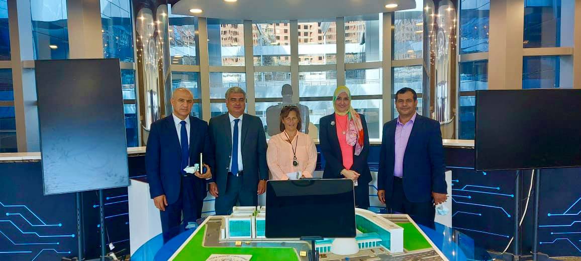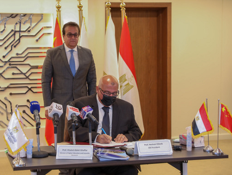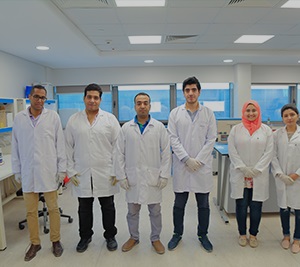


| Project Title | Nanomaterials for Electronics Applications |
| Project PI | Prof.Dr Ahmed Attia |
| Project Abstract |
Thin films of newly developed nanomaterials like silver nano-particles, and Titanium dioxide nano particles promise a price reduction for electrical energy solar cells. Aluminum Zinc-Oxide thin film is a good candidate for developing transparent conducting electrodes which are quite important for fabrication transparent circuits. Transparent conductors are commonly used in many applications like touch screens, transparent antennas and photovoltaic panels. On the other hand, conducting transparent screens are important for electromagnetic shielding. In addition, nanomaterials can also be good candidates for developing flexible electronics which have quite importance in different applications like RFID systems and Health monitoring systems.
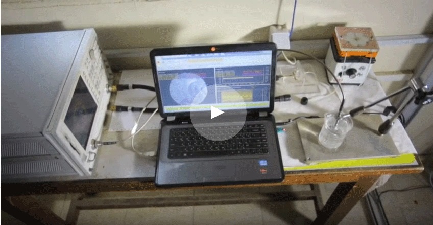
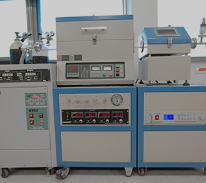
Different techniques can be used for preparing nano materials like ball milling, ultrasonic reactor and microwave reactor. In addition, other techniques are suitable for spreading nano materials into thin film like spin coating, chemical vapor deposition and microplotting.
The purpose of this project is to present an extensive study about different techniques of preparing nano materials which may be suitable for electrical engineering applications like Al-ZnO , TiO2, ZnO nano particles and measuring the electrical properties of thin films of these materials like conductivity and electromagnetic shielding. Based on the obtained properties different applications would be investigated like transparent electrodes, flexible electronics, flexible antennas, transparent antennas, transparent electromagnetic shielding screen or solar cells. In addition, it is also proposed to study the possibility of developing thin film layers of Graphene or Carbon nanotubes by using plasma enhanced chemical vapor deposition (PECVD). PECVD can be used to produce low cost thin films with high growth rate and high quality materials.
The proposed activities in this project can be summarized in the following points: - Fabrication of different nano materials suitable for electrical engineering by different techniques. - Characterization of fabricated nano materials - Developing thin films by different techniques. - Characterization of fabricated thin films. - Developing samples for different electrical engineering like: Solar cell, transparent conducting screen, transparent antenna, or flexible circuit |
| Project Objectives | 1- Manufacture of residual nano materials suitable for electrical and electronic engineering applications in various ways. |
| Project Deliverables | The purpose of this project is to present an extensive study about different techniques of preparing nano materials which may be suitable for electrical engineering applications like Al-ZnO , TiO2, ZnO nano particles and measuring the electrical properties of thin films of these materials like conductivity and electromagnetic shielding. Based on the obtained properties different applications would be investigated like transparent electrodes, flexible electronics, flexible antennas, transparent antennas, transparent electromagnetic shielding screen or solar cells. In addition, it is also proposed to study the possibility of developing thin film layers of Graphene or Carbon nanotubes by using plasma enhanced chemical vapor deposition (PECVD). PECVD can be used to produce low cost thin films with high growth rate and high quality materials.
|
| Project Beneficaries | - |